

What Are the Limitations of Using a 1-2 Layers PCB in Your Project
2026-01-23
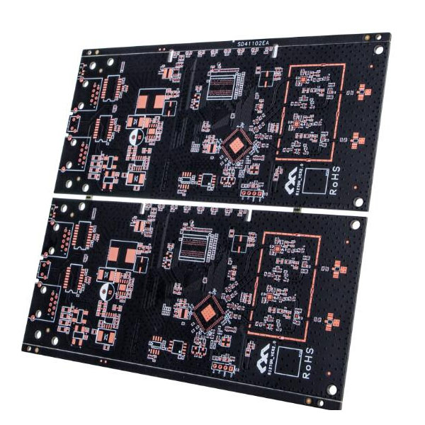
When embarking on an electronics design, the choice of your printed circuit board (PCB) stack-up is a foundational decision. Many projects start with the simplicity and cost-effectiveness of a 1-2 Layers PCB. At Akeson, we've guided countless engineers through this selection process. While single or double-sided boards are excellent for many applications, understanding their constraints is crucial to avoid performance pitfalls and ensure project success.
The primary limitations of using a 1-2 layer board stem from its inherent simplicity. Here are the key constraints to consider:
-
Limited Routing Density: With only one or two conductive layers, routing complex circuits becomes a challenge. This often forces designers to use jumper wires or larger board sizes.
-
Signal Integrity (SI) Challenges: High-speed signals or sensitive analog traces are susceptible to interference and crosstalk due to lack of dedicated ground planes and controlled impedance.
-
Power Delivery Network (PDN) Weakness: Delivering clean, stable power across the board is harder without a solid power plane, potentially leading to voltage drops and noise.
-
Thermal Management Issues: Dissipating heat from powerful components is less efficient without the thermal mass and vias that multilayer boards provide.
-
Scalability and Noise Immunity: As a design evolves or requires higher noise immunity, the 1-2 layer architecture offers little room for improvement.
The following table summarizes when a 1-2 Layers PCB might be insufficient:
| Project Requirement | Limitation in 1-2 Layer PCB |
|---|---|
| High Component Density | Limited space for trace routing, leading to larger boards or manual jumps. |
| High-Speed Digital Signals | Poor signal integrity, EMI issues, and lack of impedance control. |
| Complex Power Needs | Inefficient power distribution and increased electrical noise. |
| Strict EMC/EMI Standards | Limited shielding capabilities, making compliance more difficult. |
1-2 Layers PCB FAQ常见问题大全
Q: Can I use a 1-2 Layers PCB for a microcontroller-based project?
A: Yes, for simple, low-speed microcontroller circuits (e.g., basic Arduino projects), a 1-2 Layers PCB from Akeson is often perfectly adequate. Issues arise when the design incorporates high-speed communication (like USB, Ethernet) or numerous peripherals requiring many interconnections.
Q: How does a 2-layer PCB improve upon a 1-layer design?
A: The second layer provides critical routing flexibility. It can be used as a dedicated ground plane, significantly improving noise immunity and signal return paths, or for crossing traces that would otherwise be impossible on a single layer, reducing the need for jumpers.
Q: When should I absolutely avoid a 1-2 layer design?
A: You should consider moving to a multilayer board for RF/microwave circuits, high-speed digital designs (processors, FPGAs), products requiring stringent EMC certification, or any design where reliability under electrical noise is paramount. The team at Akeson can perform a design review to advise on the optimal stack-up.
In summary, while 1-2 Layers PCB designs are the cornerstone of simple electronics, their limitations in routing, signal integrity, and power delivery are real. Recognizing these constraints early can save significant time and cost in redesigns. Contact us at Akeson today for a expert consultation. Let our experience help you analyze your schematic and recommend the most reliable, cost-effective PCB solution for your specific project needs.