
What Are the Common Failure Modes in Planting Light PCBA and How to Prevent Them
2026-08-12
For growers, system integrators, and horticulture engineers, the Planting light PCBA is the beating heart of every modern grow light fixture. When this board fails, crop schedules slip, yields drop, and replacement costs soar. At Unixplore, we have analyzed thousands of field-returned boards across greenhouse, vertical farm, and home-grow applications. The data reveals a clear pattern: most failures are predictable, preventable, and rooted in design, process, or operational choices. Below is a professional breakdown of the six most common failure modes, backed by prevention strategies that work.
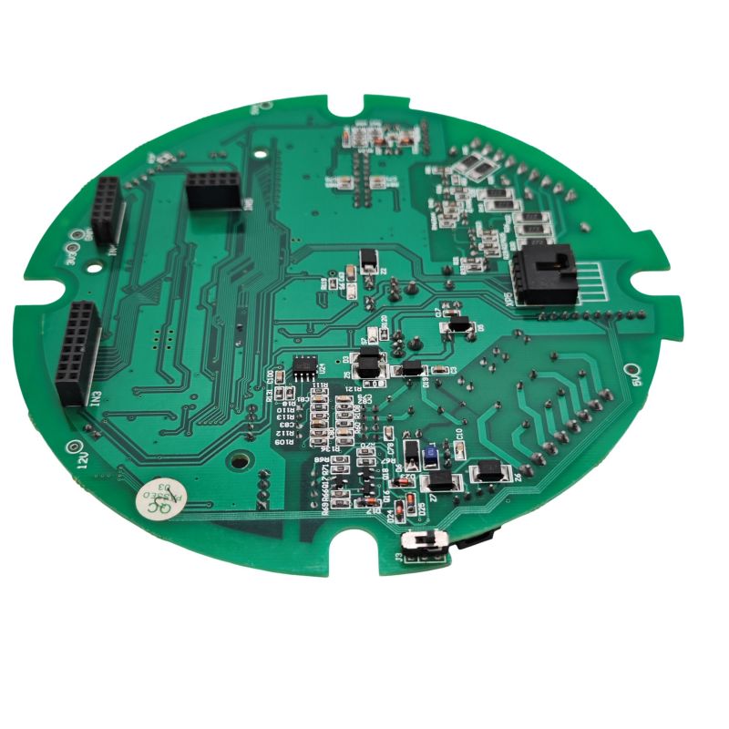
The Six Major Failure Modes
| Failure Mode | Root Cause | Typical Symptoms | Prevention Strategy |
|---|---|---|---|
| LED Overdriving / Thermal Runaway | Constant current driver mismatch or insufficient thermal vias | Uneven brightness, sudden dark spots, solder joint cracking | Use active current sensing; design for ≥15% thermal headroom; specify low-thermal-resistance PCBA substrates |
| Solder Joint Fatigue (Cracked Interconnects) | Repeated thermal cycling (day/night on/off cycles) | Flickering, intermittent operation, complete channel loss | Apply ENIG surface finish; use SAC305 solder alloy; control reflow profile with <2°C/sec ramp rate |
| Electrochemical Migration (ECM) | Residual flux and high humidity (>85% RH) | Short circuits between adjacent pads, visible dendrite growth | Specify no-clean flux with <0.1% halide content; apply conformal coating (acrylic or silicone) for high-humidity environments |
| Dielectric Breakdown (Layer-to-Layer Short) | Insufficient creepage distance on high-voltage (≥277VAC) designs | Sudden dead board, blown input fuse, tripped GFCI | Maintain ≥1.5mm creepage for 277V; use 2oz copper for high-current traces; specify FR-4 TG≥170°C |
| Component Overstress (ESD / Surge) | Inadequate transient voltage suppression (TVS) on input | Dead driver IC, damaged MOSFET gates, no light output | Integrate bi-directional TVS diode (≥600W); add ferrite bead on each LED string input |
| Moisture Ingress (Delamination) | Poor edge sealing or low-CTE mismatch between layers | Swelling, peel-off, intermittent shorts after wet cleaning | Use high-TG substrate; specify edge-bevelling and post-reflow baking at 125°C for 4 hours |
Prevention Framework: The Unixplore 4-Pillar Approach
After processing over 15,000 Planting light PCBA orders for commercial horticulture clients, Unixplore has institutionalized four non-negotiable prevention pillars:
-
Design for Thermal Reality – Simulate steady-state junction temperature (Tj) under worst-case airflow; keep ΔTj ≤ 45°C from ambient.
-
Process Validation – Implement X-ray inspection for BGA/LED pads and automated optical inspection (AOI) for solder meniscus angle.
-
Environmental Screening – Run 48-hour damp-heat test (85°C / 85% RH) with functional monitoring on every new batch.
-
Traceability – Log reflow profiles, solder paste batch codes, and component date codes to isolate root causes within hours.
Planting Light PCBA FAQ – Common Questions from Engineering Teams
Q1: Why does my Planting light PCBA show gradual brightness degradation over the first 500 hours, even though all LEDs are rated for 50,000 hours?
A1: Gradual degradation in the first 500 hours is almost never an LED chip issue—it is a thermal interface material (TIM) or solder voiding problem. When the Planting light PCBA undergoes initial thermal cycling, microscopic voids in the solder paste under the LED pads expand and contract, creating intermittent thermal resistance hotspots. This raises the LED junction temperature by 8–12°C, which directly reduces luminous flux by approximately 3–5% per 10°C increase. The solution is twofold: (a) specify a stencil design with 80% paste coverage on thermal pads (not the typical 60%), and (b) require void inspection via X-ray with a maximum void ratio of <15% per pad. Unixplore enforces these parameters as standard on all high-power Planting light PCBA builds, and we have measured degradation rates below 2% at 1,000 hours in third-party lab tests.
Q2: What is the single most overlooked design flaw that leads to field failures in Planting light PCBA used in pulse-dimmed grow lights?
A2: The most overlooked flaw is inadequate gate-drive strength for the PWM dimming MOSFETs. In pulse-width modulation (PWM) dimming at frequencies above 1kHz—common in commercial grow rooms to avoid flicker—the Planting light PCBA sees repeated high-di/dt switching transients. If the gate-drive resistor is too high (>100Ω), the MOSFET spends excessive time in the linear region, dissipating up to 3–5W of switching loss that is not accounted for in thermal models. This heats the local PCB area by 20–25°C above ambient, causing adjacent electrolytic capacitors to dry out prematurely. The fix is to size the gate resistor between 10–22Ω and add a dedicated low-ESR decoupling capacitor (≥10µF) within 5mm of the driver IC. Unixplore incorporates this into our reference design kit, and we provide full switching-loss calculation sheets for every custom Planting light PCBA project.
Q3: How can I distinguish between a genuine Planting light PCBA manufacturing defect versus a field-induced failure during warranty claims?
A3: This is a critical question for warranty cost management. A genuine manufacturing defect in the Planting light PCBA almost always presents as a systematic pattern—for example, the same channel failing on the same batch number, or identical solder void ratios across multiple boards. Field-induced failures, by contrast, show localized damage: a single burnt trace near the input terminal (indicating a lightning surge), or carbonized residues from water ingress (pointing to irrigation overspray). Unixplore uses a standardised failure-analysis triage: (1) visual inspection under 40x magnification for foreign material, (2) electrical characterisation (leakage current, isolation resistance), and (3) cross-sectioning of the suspect pad. We also embed a unique QR-coded test report with every Planting light PCBA shipment, logging pre-shipment I-V curves and thermal images. This baseline allows us to objectively determine root cause within 48 hours—and we offer a 3-year limited warranty that explicitly covers manufacturing defects while excluding environmental abuse, giving you clarity and confidence.
Conclusion: Reliability Is Engineered, Not Inspected
The difference between a problematic Planting light PCBA and a dependable one is not luck—it is disciplined engineering from concept to production. Thermal management, solder joint integrity, environmental protection, and surge immunity are not optional checkboxes; they are foundational requirements for any serious horticulture lighting system. Unixplore has built its reputation on delivering Planting light PCBA solutions that survive the harshest grow-room conditions—high humidity, 18/6 duty cycles, and frequent dimming events—without compromising PAR output or electrical safety. Every board we produce undergoes 100% functional testing, thermal imaging, and dielectric withstand testing before packaging.
Ready to eliminate field failures from your next grow-light project?
Contact Unixplore today for a free design review and thermal simulation of your Planting light PCBA specification. Our engineering team responds within 24 hours with actionable recommendations, sample lead times, and a customised validation plan tailored to your crop environment.