

How Are Microvias Manufactured in High Density Interconnect PCBs
2026-03-09
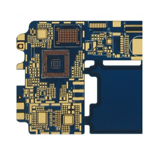
The manufacturing of microvias is a cornerstone process in the production of HDI PCB (High Density Interconnect Printed Circuit Board) technology. As devices shrink and functionality expands, understanding how these microscopic structures are created is essential for engineers and procurement specialists. At Akeson, we specialize in advanced PCB fabrication, ensuring that every microvia meets the highest standards of reliability and performance.
The Microvia Manufacturing Process
Microvias are minuscule holes drilled in HDI PCB substrates that create electrical connections between different layers. Unlike traditional through-hole vias, microvias typically have a diameter of 150 micrometers or less. The creation of these structures involves several precise steps, which vary depending on the volume and design complexity.
Primary Manufacturing Methods
| Method | Description | Typical Application |
|---|---|---|
| Laser Drilling | Uses CO2 or UV lasers to ablate dielectric material | Most common for high-volume HDI PCB production |
| Photo Via | Uses photosensitive dielectric and photolithography | Ideal for very fine features and high-density designs |
| Plasma Etching | Uses plasma to remove material uniformly | Suitable for specialized materials and blind vias |
Step-by-Step Laser Drilling Process
The most prevalent method for creating microvias in an HDI PCB is laser drilling. The process can be broken down as follows:
-
Layer Preparation: A copper foil and a layer of dielectric material (such as RCC or prepreg) are laminated onto the core substrate.
-
Copper Thinning: The copper surface is often micro-etched to create a rougher surface, which aids in laser absorption.
-
Laser Ablation: A focused laser beam is directed at the target locations. The energy vaporizes the dielectric material, stopping precisely at the underlying copper pad. This creates the microvia hole.
-
Desmear and Cleaning: The drilled panel undergoes a chemical process to remove any residual resin (smear) from the hole interior and the target pad.
-
Metallization: The holes are cleaned and then plated with copper through an electroless and electrolytic plating process, forming the conductive barrel of the microvia.
Key Considerations for Quality Microvias
At Akeson, we emphasize that the reliability of an HDI PCB is directly tied to the quality of its microvias. Several factors are critical:
-
Aspect Ratio: The ratio of the hole depth to its diameter must be controlled to ensure consistent copper plating.
-
Target Pad Accuracy: The laser must be perfectly aligned to hit the target pad below without damaging it.
-
Dielectric Material: Different resins react differently to laser energy, requiring precise calibration.
HDI PCB FAQ
What is the difference between a blind via and a buried via in an HDI PCB?
A blind via connects an outer layer of the HDI PCB to one or more inner layers but does not go through the entire board. It is "blind" because you cannot see through it from the opposite side. A buried via, on the other hand, connects two or more inner layers together and is completely hidden within the board structure, not visible from either outer surface. Both types are typically constructed using the microvia manufacturing processes described above to save space and improve routing.
Why is laser drilling preferred over mechanical drilling for microvias in HDI PCBs?
Mechanical drill bits are prone to breaking and wear when attempting to create holes smaller than 200 micrometers. Furthermore, they cannot reliably stop at an inner layer to create a blind via. Laser drilling offers a non-contact method that can consistently produce holes as small as 50 to 75 micrometers. It provides the precision required to ablate the dielectric material and stop precisely on the target copper pad, which is essential for the reliability and density of modern HDI PCB designs.
How does the microvia manufacturing process impact the cost of an HDI PCB?
The cost is influenced by several factors within the microvia manufacturing process. First, the laser drilling equipment has a high capital cost and requires precise calibration. Second, the sequential lamination cycles required to build up layers with buried and blind vias add to the processing time and complexity. Third, the yield rate is critical; defects in microvia formation, such as voids in copper plating, can render the entire board useless. Therefore, while microvias enable miniaturization, they also represent a significant portion of the manufacturing cost, necessitating a partner like Akeson who can optimize these processes for high yield.
Conclusion and Contact Us
Mastering the intricacies of microvia manufacturing is what separates a standard board from a high-performance HDI PCB. From laser drilling parameters to plating chemistry, every detail matters. At Akeson, we leverage state-of-the-art equipment and decades of engineering experience to deliver HDI PCB solutions that you can rely on for your most demanding applications.
Are you ready to bring your next high-density design to life? Contact us today for a consultation and a detailed quote. Let Akeson be your partner in advanced PCB technology.